Some basics to help review your knowledge in electrical, Electronics and DLC. Suitable for ECE, EEE, EIE and related circuit branches.
(.zip - 9MB)

All Engineering study materials
S. No.
|
D-MOSFET
(n-channel)
|
E-MOSFET
(n-channel)
|
1.
|
Negative
voltage at gate
|
Positive
voltage at gate
|
2.
|
Positive
charges on the semiconductor site
|
Negative
charges on the semiconductor site
|
3.
|
Depletion
of majority carriers
|
Inversion
layer is formed
|
S. No.
|
JFET
(n-channel)
|
MOSFET
(n-channel)
|
1.
|
Between
Gate and channel is a PN junction forming a diode
|
Between
gate and channel is an insulating SiO2 layer forming a small capacitor
|
2.
|
Gate
is reverse biased (negative voltage for n-channel)
|
Gate
can be given positive or negative voltage depending on mode of operation
required
|
3.
|
High
input impedance due to reverse biased gate
|
Very
high impedance due to insulated gate and capacitance effect
|
4.
|
Operated
only in depletion mode
|
Operated
in depletion and enhancement mode
|
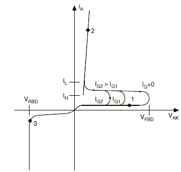 During turn-on, the minimum value of anode current that must be attained so that the thyristor wil
S. No.
|
Shockley Diode
|
SCR
|
TRIAC
|
DIAC
|
1.
|
Uni-directional
device
|
Uni-directional
device
|
Bi-directional
device
|
Bi-directional
device
|
2.
|
No
gate terminal
|
Gate
terminal is present
|
Gate
terminal is present
|
No
gate terminal
|
3.
|
Basic
4 layer device
|
Shockley
diode with gate terminal
|
Two
SCRs in Inverse-parallel connection
|
Two
Shockley diodes in Inverse-parallel connection
(OR)
Low
current TRIAC without gate terminal
|
4.
|
Terminals:
Anode
and Cathode
|
Anode,
Cathode and Gate
|
Main
terminal1, Main terminal2 and Gate
|
Main
terminal1 and Main terminal2
|
5.
|
Break-over
voltage cannot be controlled
|
Break-over
voltage can be controlled with gate signal
|
Break-over
voltage can be controlled with gate signal
|
Break-over
voltage cannot be controlled
|